The Cutting Edge Without the Cutting: Why the Future of AI Hardware is Grown in Orbit
Silicon manufacturing is brute force. Diamond manufacturing in space is a revolution of elegance. The next industrial…
Silicon manufacturing is brute force. Diamond manufacturing in space is a revolution of elegance. The next industrial revolution requires us to stop carving stone and start growing crystals.
If you were to shrink yourself down to the size of an atom and stand on the surface of a modern computer chip, you would be standing in the aftermath of a war zone.
We tend to think of microchips as pristine, perfect objects. In reality, a silicon chip is the result of one of the most violent, energy-intensive, and chemically aggressive manufacturing processes humans have ever devised. It is a triumph of brute force over nature.
For sixty years, Moore’s Law has been sustained by our ability to carve ever-smaller canyons into silicon rock. But we are reaching the physical limits of the stone. We are running out of atoms to cut. We are reaching the physical limit of the atomic structures. There is no quantum of solace.
To understand why the future of computing lies 400 kilometres overhead, we first need to understand the miraculous, messy, and increasingly impossible process of making an even finer chip on Earth.
The Earth Method: The Violence of Subtraction
Modern semiconductor manufacturing is fundamentally Subtractive. It is the art of sculpture. You start with a block of material and you cut and chisel away everything that isn’t a statue.
1. The Birth of the Boule (and the Gravity Tax)
It begins with the Czochralski process. We melt hyper-pure silicon at 1,400°C in a quartz crucible. We dip a seed crystal into this molten magma and slowly pull it upwards, rotating it to draw out a single, massive cylindrical crystal called a “boule”.
This is where the problems begin. On Earth, gravity creates convection. The molten silicon swirls with turbulence. Hot liquid rises, cold sinks. This microscopic chaos creates defects in the crystal lattice. It causes oxygen from the quartz crucible to leach into the silicon. Billions are spent on magnetic fields just to try and dampen this turbulence, but we can never truly stop it. The gravity tax is paid before the chip is even born. It is a VAT. And yield is limited.
2. The Saw and the Grind
We then take this massive crystal salami and slice it with diamond saws into wafers less than 1mm thick. This is a traumatic and precarious process for the crystal. The surface is shattered and rough. So, the aftermath has to go through chemical mechanical polishing (CMP)—effectively a high-tech sander with corrosive slurry—to grind it down to atomic flatness. Switch from quarry pick to sander. Still brute force.
3. The Light Chisel (EUV Lithography)
Then comes the “printing”. To create the billions of transistors on an NVIDIA H100, Extreme Ultraviolet (EUV) Lithography has to be utilised.
This is one of the most complex machines ever built by humans (made by ASML). It works by firing a high-power laser at a droplet of molten tin, vaporising it into plasma that emits EUV light. This light is reflected off mirrors so smooth that if they were the size of Yunnan Province, the biggest bump would be less than a millimetre high.
The light hits the wafer, which is coated in a light-sensitive chemical called “photoresist”. It burns the pattern of the circuit into the chemical.
4. The Acid Bath
Finally, etching starts. Chipmakers dunk the wafer into harsh acids or blast it with plasma. The acid eats away the silicon where the photoresist was burned away, digging the “trenches” that form the transistors.
Think about this process: Melt. Pull. Saw. Grind. Burn. Dissolve. A stunt Tom Cruise will say no to.
It is aggressive. It is wasteful. And as we push towards 3nm (nanometre) and 2nm nodes, it is becoming precarious. At 2nm, a transistor gate is only about 10 atoms wide. If the acid eats one atom too many, the chip is dead. If gravity caused a single defect in the crystal lattice at that spot, the chip is dead. Emotional damage. That is why wafer fabrication yield is hard to go up and one Asian company dominates the painstaking process.
We are trying to paint the Mona Lisa with a sledgehammer. And we have run out of canvas. And brushes.
The Space Method: The Elegance of Growth
If Earth manufacturing is about Subtraction (carving away the bad), Space manufacturing is about Addition (growing only the good, nothing ugly here).
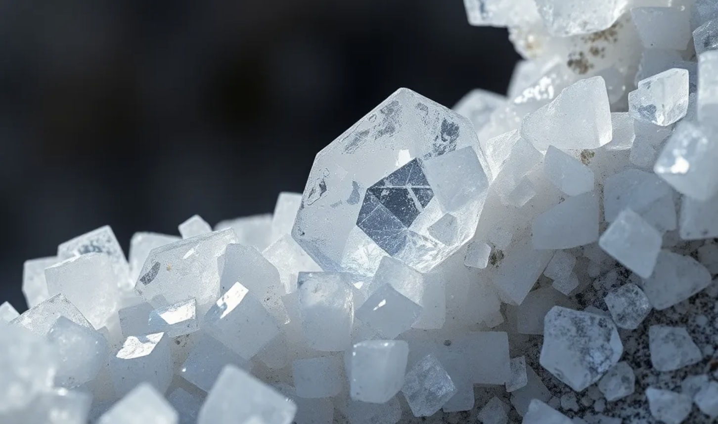
We need a shift from Silicon—a material that tolerates the vacuum of space poorly—to Diamond, the hardest, most thermally conductive material in nature. But more importantly, we need a shift in how we build.